
TL;DR

Get the latest gadgets delivered free with Prime
- Fast, free delivery on millions of items
- Prime Video, Amazon Music and more included
- Member-only deals all year
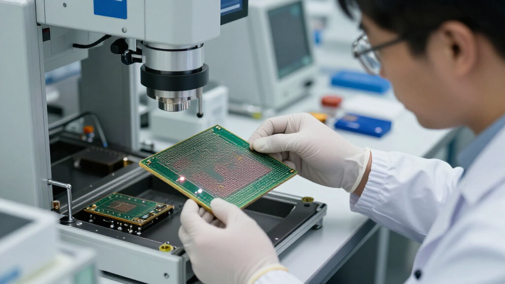
Intel has commenced the shipment of silicon wafers produced using high-NA EUV lithography. This development signals progress in cutting-edge chip manufacturing and could impact the semiconductor supply chain.
Intel has begun shipping silicon wafers manufactured with high-NA extreme ultraviolet (EUV) lithography technology, marking a major milestone in advanced semiconductor fabrication. This development confirms Intel’s progress in adopting next-generation lithography tools to produce smaller, more powerful chips, which is critical for maintaining competitiveness in the industry.
According to Intel, the shipment includes wafers produced using high-NA EUV equipment supplied by ASML, a leading lithography equipment manufacturer. This technology allows for finer patterning at smaller nodes, potentially enabling Intel to produce chips with higher performance and lower power consumption. The shipments are targeted at select customers and partners for testing and validation, with broader commercial production expected later in 2024.
Intel’s move follows years of development and investment in EUV technology, which has faced delays and technical challenges. The high-NA EUV tools feature a larger numerical aperture, allowing for more precise patterning on wafers. Intel has not disclosed specific production volumes or detailed timelines but emphasizes that this marks a significant step toward mass production using high-NA EUV.
Implications for Semiconductor Manufacturing Leadership
This development underscores Intel’s commitment to leading-edge manufacturing processes and could give the company a competitive edge in chip performance and efficiency. High-NA EUV is considered essential for scaling below the 3nm node, which is crucial for future technology nodes. Successful deployment may influence industry standards and supply chain dynamics, especially as other chipmakers also pursue high-NA EUV adoption.
EUV lithography semiconductor equipment
As an affiliate, we earn on qualifying purchases.
As an affiliate, we earn on qualifying purchases.
Progress and Challenges in EUV Lithography Adoption
High-NA EUV lithography has been in development for several years, with ASML’s equipment being the primary supplier. The technology promises to extend Moore’s Law by enabling finer patterning at smaller nodes, but it has faced technical hurdles related to equipment complexity and cost. Intel has been investing heavily in EUV since the early 2010s, aiming to overcome these challenges and bring high-NA EUV into mainstream manufacturing.
Previous industry milestones include the first commercial EUV lithography tools from ASML and early pilot production runs at other leading chipmakers like TSMC and Samsung. Intel’s latest shipment indicates it is now entering a critical phase of integrating high-NA EUV into its production lines, a process that could influence the broader industry trajectory.
“We are proud to announce that Intel has begun shipping wafers produced with high-NA EUV lithography, marking a significant step in our advanced manufacturing roadmap.”
— Intel spokesperson
Details on Production Volume and Deployment Timeline
While Intel has confirmed the shipment of wafers using high-NA EUV, specific details about production volumes, the timeline for broader deployment, and the exact performance improvements remain undisclosed. It is also unclear how quickly Intel plans to scale this technology across its manufacturing facilities or how it compares to competitors’ progress in the same area.
Next Steps for Intel’s High-NA EUV Manufacturing
Intel is expected to continue testing and validating wafers produced with high-NA EUV, with broader commercial production anticipated later in 2024. The company may also begin integrating this technology into its main production lines, aiming to meet upcoming process node goals. Industry analysts will be watching closely for updates on production capacity, performance benchmarks, and how other chipmakers respond.
Key Questions
What is high-NA EUV lithography?
High-NA EUV lithography is an advanced chip manufacturing technique that uses a larger numerical aperture in EUV tools to enable finer patterning on silicon wafers, crucial for smaller, more powerful chips.
Why is this development important for Intel?
Shipping wafers with high-NA EUV indicates Intel’s progress toward next-generation manufacturing nodes, potentially offering higher performance and efficiency in future chips.
When will high-NA EUV be used in mass production?
Intel has indicated broader deployment could occur later in 2024, but specific timelines for full-scale manufacturing are not yet confirmed.
How does high-NA EUV compare to previous EUV technology?
High-NA EUV features a larger numerical aperture, allowing for finer patterning at smaller nodes, which is more challenging with earlier EUV tools but essential for future technology scaling.
What are the challenges associated with high-NA EUV?
The technology involves complex equipment, higher costs, and technical hurdles related to equipment precision and stability, which have delayed widespread adoption.
Source: hn
Fall Picks
fall essentials
As an affiliate, we earn on qualifying purchases.