
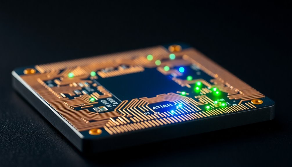
3‑nanometer chips will make your mobile devices faster, more energy-efficient, and better at handling advanced AI and graphics tasks. They reduce power consumption by up to 50%, extending battery life while enabling improved processing speeds and responsiveness. With higher transistor density, your devices can run more complex applications and offer enhanced gaming and multimedia experiences. Although thermal management becomes more challenging, innovative solutions are making smaller chips more reliable. To discover how these changes will shape your mobile experience, keep exploring.
Key Takeaways
- Significantly improves power efficiency, extending device battery life by up to 50%.
- Enables faster processing speeds and higher transistor density for smoother multitasking and gaming.
- Enhances graphics with real-time ray tracing and AI-driven visual optimization for immersive experiences.
- Supports advanced sensors and AI capabilities, facilitating smarter, more responsive mobile applications.
- Promotes smaller, more capable devices with integrated functionalities, driving innovation across mobile technology.
Dramatic Gains in Power Efficiency and Battery Life

3-nanometer chips deliver significant improvements in power efficiency, which directly extend your device’s battery life. They reduce power consumption by 25–30% compared to 5nm chips while maintaining the same speed, with Samsung’s first-generation 3nm process achieving up to 45% lower power use. The second generation further cuts consumption by up to 50%. This efficiency gain comes from the Gate-All-Around (GAA) transistor architecture, which requires lower supply voltages, and the ability to optimize nanosheet channel widths for better power management. As a result, your phone or wearables last longer between charges. Reduced power use also means less heat, helping preserve battery health over time. These advancements make your devices more energy-efficient without sacrificing performance or features. Enhanced technology enables even more precise control over power distribution, further boosting efficiency and device longevity. Additionally, the power management techniques employed are rooted in advanced transistor designs that improve overall device stability and lifespan. Improved thermal management also plays a vital role in sustaining device performance and longevity.
Accelerated Processing Speeds for Mobile Devices

Thanks to the power efficiency gains from 3 nm chips, mobile processors now achieve higher clock speeds and faster data processing. They can deliver up to 10–15% faster speeds compared to 5 nm chips at the same power level, thanks to shorter gate lengths and smaller transistor dimensions. This means your device can execute instructions more quickly, handling demanding apps and multitasking without lag. Reduced transistor sizes lower latency, enabling faster communication between components and smoother performance. Enhanced transistor density allows for more parallel operations, boosting responsiveness for gaming, streaming, and real-time tasks. Apple’s M3 chip exemplifies these improvements, offering faster processing and better overall performance. These speed boosts open new possibilities for mobile computing, making your devices more powerful and efficient. Additionally, the increased transistor density enhances performance and allows for more complex processing tasks to be handled simultaneously.
Increased Transistor Density Enables More Complex Functionality
As transistor density increases, chip designers can pack more functional units into the same space, enabling more sophisticated mobile processors. With 3 nm technology, you can include advanced AI accelerators, security modules, and additional DSP cores without enlarging the chip. The higher density also allows for heterogeneous integration—logic, SRAM, and analog components on a single die—improving versatility. FinFlex technology offers design flexibility, letting you tailor performance and power by mixing transistor fin widths regionally. This increased transistor count supports features like enhanced sensor processing and multimedia handling at low power. Additionally, the AI security provided by advanced features can improve user satisfaction and device reliability. Moreover, the integration of Vetted – Flat Iron Bike components with high transistor density can lead to more compact and efficient designs. By leveraging transistor miniaturization, chip manufacturers can further optimize performance and energy efficiency. Overall, the dense 3 nm process makes your mobile devices more capable, incorporating richer functionality while maintaining compact size and energy efficiency.
Enhanced Graphics and Gaming Experiences

With the increased transistor density enabled by 3 nm technology, mobile chips can deliver dramatically improved graphics performance. You’ll notice hardware-accelerated ray tracing, which creates realistic lighting, shadows, and reflections in games and apps. The M3 GPU is 65% faster than previous models, allowing for smoother gameplay and richer visuals. It also consumes nearly half the power, extending your device’s battery life during intense gaming sessions. Thanks to advanced GPU architectures, complex scenes with detailed textures and effects become possible without sacrificing performance. Features like mesh shading and integrated ray tracing support more realistic visuals, immersing you deeper into virtual worlds. Additionally, AI-enhanced graphics can optimize rendering processes and adapt visuals in real-time to improve overall quality. These new chip architectures enable faster rendering, better graphics, and more immersive experiences, elevating mobile gaming and multimedia to new levels of quality. The integration of power efficiency techniques ensures that these high-performance capabilities do not compromise your device’s battery life, making mobile gaming more sustainable. Moreover, ongoing research into AI integration in chip design promises further enhancements in real-time graphics processing and efficiency.
Pioneering AI Capabilities on Mobile Platforms

The increased transistor density enabled by 3 nm technology allows mobile chips to incorporate more AI-specific processing units, markedly boosting their on-device intelligence. With more transistors, you get enhanced parallel processing, critical for running complex AI workloads efficiently. Compared to 7 nm chips, 3 nm processors like Apple’s M3 pack more transistors into smaller dies, improving AI compute power and energy efficiency. This means longer battery life and less heat during intensive AI tasks like facial recognition or natural language processing. The chips also enable local AI inference, reducing reliance on cloud services and improving privacy. Faster Neural Engines accelerate AI computations, supporting real-time features such as image enhancement and predictive typing. Additionally, the high transistor count facilitates remote collaboration capabilities by enabling faster data processing and sharing, which is essential for modern AI-driven applications. Moreover, the integration of advanced manufacturing processes enhances the overall performance and longevity of mobile devices. These innovations are paving the way for a new era of mobile AI that is smarter and more responsive, transforming user experiences worldwide. As a result, chip optimization techniques are becoming increasingly vital to maximize these benefits and meet the demands of next-generation mobile computing. The adoption of nanometer-scale technology also contributes to smaller, more power-efficient chips, further advancing mobile AI capabilities. Overall, 3 nm tech elevates mobile AI, delivering smarter, more responsive, and energy-efficient experiences.
Faster Adoption in Premium Smartphones and Tablets
By 2025, over 80% of premium smartphones are expected to feature 3nm chips, reflecting rapid market adoption in high-end devices. Major manufacturers like Apple and Samsung will primarily include this advanced technology, driven by early 2023 launches and increasing availability through 2024 and 2025. The high manufacturing costs initially limit adoption to flagship models, with exclusive capacity allocations, such as Apple’s partnership with TSMC, ensuring premium devices lead the way. The performance gains—up to 15% faster processing or 30% lower power consumption—make these chips highly attractive for premium phones and tablets. Enhanced graphics and processing power support demanding applications. Ultimately, the superior power efficiency and performance benefits will make 3nm chips the standard for high-end mobile devices within a few years. Understanding manufacturing costs is crucial for appreciating how early adoption phases influence the market, especially given the complex manufacturing process involved in creating such advanced chips.
Broader Use in Data Centers and High-Performance Computing

As 3-nanometer chips become more prevalent, their performance and efficiency gains are transforming data centers and high-performance computing (HPC). Their higher transistor density boosts complex computations per watt, ideal for AI and machine learning workloads. You’ll see performance improvements of 11–32% and energy savings of 12–30%, lowering operational costs in hyperscale data centers. FinFlex technology allows mixed-cell designs, optimizing speed and power for diverse cloud-native applications. The integration of 3nm SerDes and interconnects accelerates data transfer between servers and storage. Lower leakage currents sustain high performance under heavy loads, reducing thermal throttling. Data centers benefit from denser, faster chips supporting larger AI models, exascale supercomputers, and real-time edge processing—advancing infrastructure, efficiency, and capacity across the industry.
Revolutionizing Automotive and IoT Technologies
Advances in 3-nanometer chip technology are driving a new era for automotive and IoT systems, delivering unmatched performance and energy efficiency. With these chips, you can expect smarter, safer vehicles equipped with advanced autonomous driving systems, digital cockpits, and seamless connectivity. They support enhanced Driver-Assistance Systems (ADAS), enabling better sensor fusion and decision-making, while meeting strict automotive reliability standards. In electric vehicles, 3-nm chips cut power consumption by up to 30%, helping extend battery life and manage thermal challenges. For IoT devices, they allow for densely packed, highly capable sensors and modules that process data locally, reducing latency and increasing security. This technology also facilitates scalable, modular automotive architectures, enabling rapid software updates and more integrated control systems.
Overcoming Thermal Challenges With Smaller Chip Sizes
Thermal management becomes increasingly critical as chip sizes shrink to 3 nanometers because higher transistor density leads to localized heating and potential performance issues. With components packed tightly, heat can concentrate, risking overheating that affects reliability and efficiency. To combat this, advanced cooling systems and innovative materials are essential for effective heat dissipation. Traditional FinFET technology is nearing its limits, prompting the development of next-generation transistors like GAA (Gate-All-Around), which offer better thermal control. Managing heat isn’t just about chip design; it requires system-level strategies and precise manufacturing processes. Addressing these thermal challenges increases complexity and cost but is indispensable to ensure peak performance, power efficiency, and longevity of mobile devices using 3nm chips.
Setting New Standards for Innovation and Device Capabilities

The introduction of 3nm chips sets a new standard for innovation and device capabilities by considerably boosting transistor density, which enables more complex and powerful computing functions. With about 33% more transistors than 5nm chips, you can expect enhanced processing power and smarter AI applications. These chips also deliver up to 30% power savings at the same speed, extending your device’s battery life. Performance improves with speeds up to 15% faster, handling demanding tasks smoothly. Advanced manufacturing techniques like nanolithography ensure high yields and reliability. Additionally, 3nm chips support cutting-edge AI, IoT, and 5G integration, fueling innovation across industries. As a result, your devices become more capable, compact, and energy-efficient, setting new benchmarks for what’s possible in mobile computing.
Frequently Asked Questions
How Do 3nm Chips Impact Long-Term Device Sustainability and Environmental Factors?
You’ll find that 3nm chips boost device sustainability by extending battery life and reducing energy use during operation. Their smaller size means lighter, more durable devices with longer lifespans, cutting down electronic waste. Plus, their efficiency helps lower overall carbon emissions. However, manufacturing these advanced chips requires significant resources and energy, so you’ll want to contemplate the environmental impact of production alongside their long-term benefits.
What Manufacturing Challenges Are Associated With Scaling 3nm Chip Production?
You face significant manufacturing challenges with 3nm chip production. EUV lithography at this scale requires extreme precision, pushing current tools to their limits and causing bottlenecks. Yield rates are still low, mainly due to defect sensitivity and complex transistor structures. Power leakage and thermal issues increase, demanding new designs and materials. Additionally, the complexity of layout and signal integrity demands advanced design tools, making scaling to mass production a complex, resource-intensive process.
How Will 3nm Technology Influence the Cost of Future Mobile Devices?
Imagine holding a sleek, powerful mobile device that’s smarter and more efficient. That’s how 3nm technology influences future device costs. While early versions will carry premium prices due to high manufacturing costs, as production scales up, costs will drop. You’ll eventually see more affordable devices with advanced features, thanks to improved performance and efficiency. So, initially pricey, but over time, 3nm tech promises more accessible, cutting-edge mobile experiences.
Are 3nm Chips Compatible With Existing Mobile and Computing Architectures?
You might wonder if 3nm chips fit into current mobile and computing architectures. They are compatible because TSMC’s N3P process preserves existing design rules and IP, making integration smoother. Plus, technologies like FinFlex offer flexibility, allowing mixing of different fin counts within a single chip. While some physical constraints exist, these chips are designed to work with existing systems, ensuring easier adoption and upgrades.
What Are the Cybersecurity Implications of Increased Processing Power in 3nm Devices?
You should be aware that increased processing power in 3nm devices raises cybersecurity concerns. It expands the attack surface, making them more vulnerable to hackers. Faster data processing can enable sophisticated attacks, while advanced encryption might be both a security boost and a target. Additionally, reliance on these chips heightens risks if supply chains are compromised. Stay vigilant, as malicious actors could leverage this power for AI-driven threats and complex cyberattacks.
Conclusion
Think of 3-nanometer chips as the rocket fuel propelling your devices into a new era. With faster speeds, longer battery life, and smarter features, you’ll experience mobile computing like never before. These tiny marvels *unleash* a universe of possibilities, transforming everything from gaming to AI. As they push the boundaries of innovation, you’ll be at the forefront of a technological revolution—ready to explore the infinite horizons ahead.